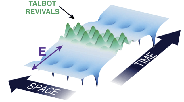
In 1924, Louis-Victor Pierre Raymond, pair of France and Duke of Broglie, astonished his contemporaries in proposing that electrons behave as waves, when moving along spatial dimensions of a few millionths of a milimeters. These distances, dubbed nanometers, remained technologically unaccessible until some decades ago. Roughly speaking, if the electrons appear as waves under these circumstances, we should expect their behaviour close to that of light. One of the most obvious manifestations of the wave nature of light is diffraction, the modification of its structure when passing through small slits. In 1836, the british physicist Henry Fox Talbot observed an extraordinary remarkable diffraction phenomenon: when light passes through a mask composed by a regular disposition of slits, it forms an image of the slits at some particular distances from the mask. This image if formed spontaneously, without he use of any focalizing element as lenses or mirrors. Our study predicts theoretically that this very same effect arises in the electron waves, if the electrons are detached from a periodic crystal due to the interaction with an electromagnetic field. The Talbot imaging effect would allow to control the shape of the electron wave and, therefore, some of the properties of their emission of light. Almost magically, the spatial structure of the Talbot image is codified in the temporal structure of the light emission. All this, of course, at nanometric scales!. More info at: [1]
A. García-Cabrera, C. Hernández-García, and L. Plaja, Ultrafast Sub-Nanometer Matter-Wave Temporal Talbot Effect, New Journal of Physics 23, 093011 (2021).
Download in Gredos Universidad de Salamanca http://hdl.handle.net/10366/147197
Leave a Reply